レーザーナノファクトリー

フェムト秒レーザーによる2光子プロセス超微細光造形3Dプリンター。
選択的レーザーエッチング、レーザーアブレーション、多光子重合

問い合わせ

3D微細加工ソリューション

多光子重合

レーザー
アブレーション

ハイブリッド製作

選択的レーザー
エッチング

アプリケーション

biotechnologies

バイオテクノロジー

フェムト秒レーザーを用いた3D多光子重合は、あらゆる材料から複雑な機能構造を持つマイクロスキャホールドを作製するのに適しています。

femtika optics

光学とフォトニクス

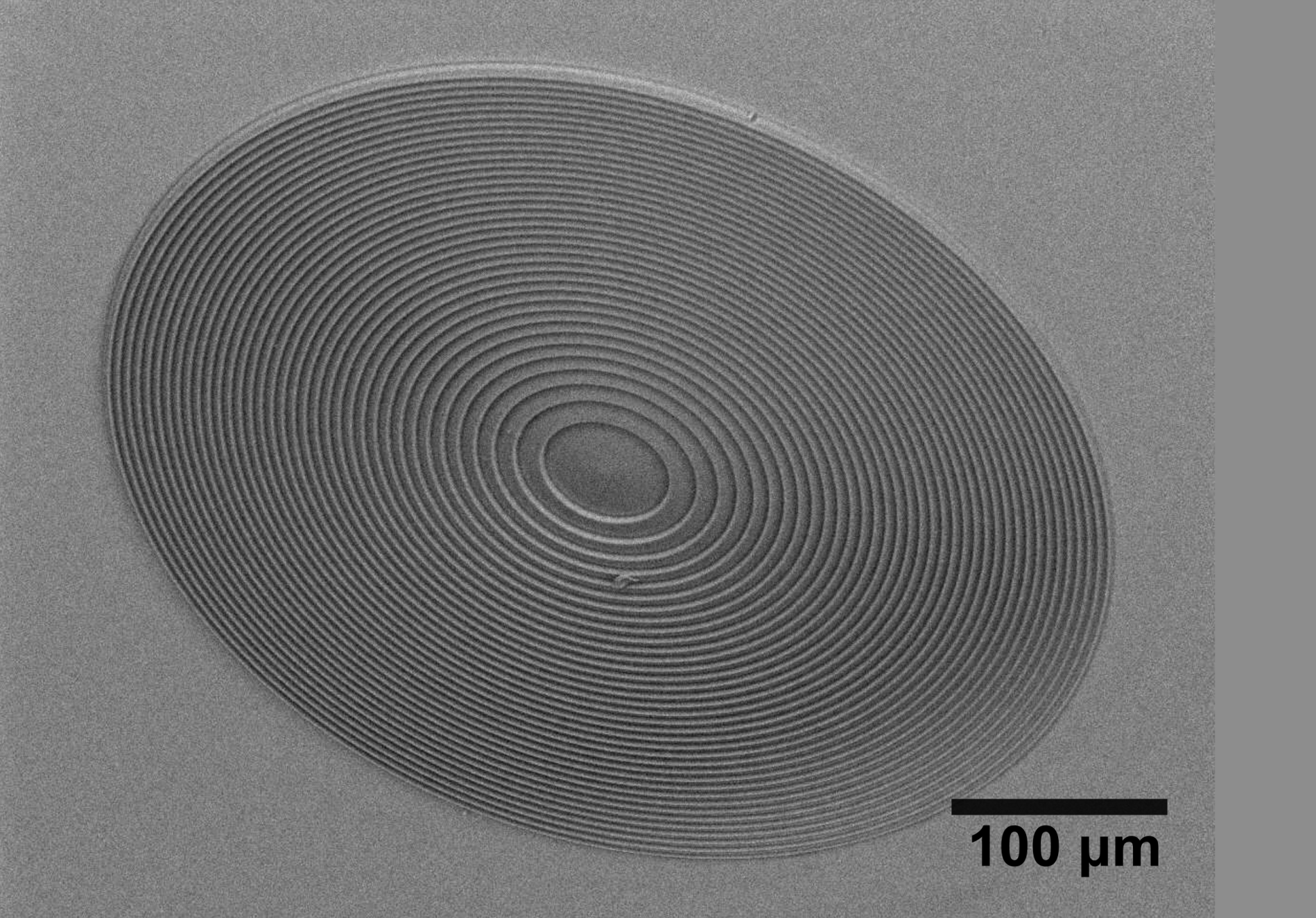
可視および赤外スペクトルの高解像度(数百nmまで)の光学デバイスを製造します。光学用途に適したマイクロレンズ表面の任意の形状プロファイルにより、収差やベッセルビームや光学渦などのエキゾチックな光分布を最小化します。
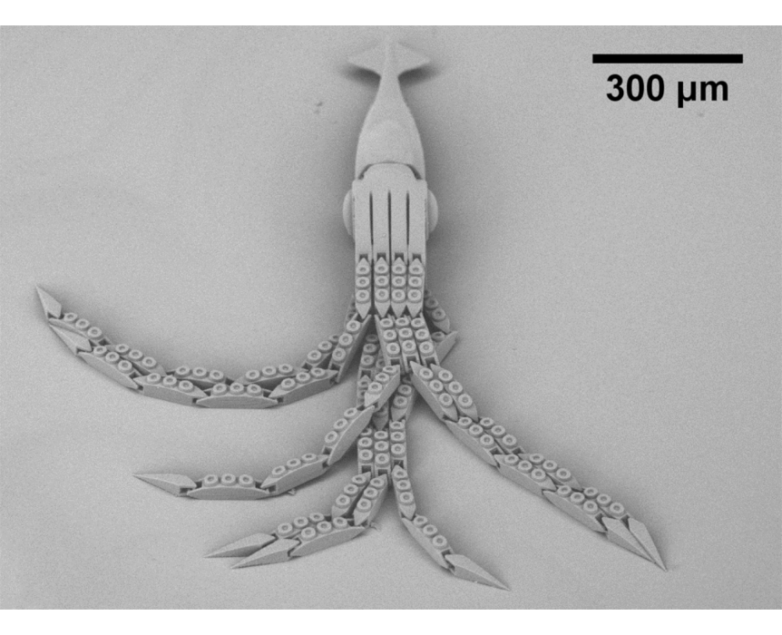
femtika medicine

医薬

フェムト秒レーザー3Dマイクロマシニングは、医療機器製造に新たな可能性をもたらします。セルサイズで制御可能な形状を持つ物体を製造することができます。新世代医療機器、セル穿孔機、マイクロロボットなどの製作が可能です。医療機器の設計・製作の全く新しい可能性を実現します。
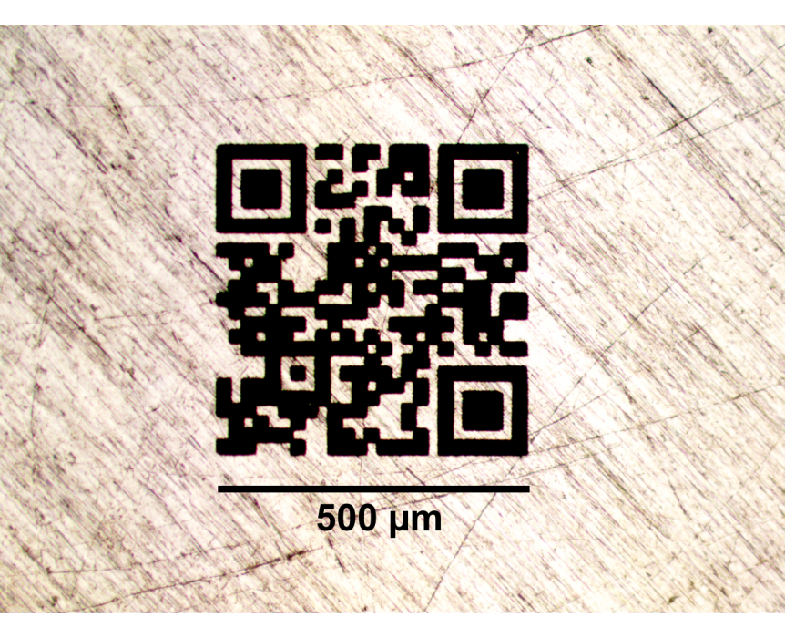
medical marking

医療機器のレーザーマーキング

インダストリー4.0のパラダイムでは、個々のデバイスの機能を追跡し、偽造を避けることが必要になっています。ナノファクトリーでは、任意の材料に数ミクロンのQRコードを作成することができます。マーキングエリア外での熱損傷やその他の副作用がなく、マーキング後の医療機器やコンポーネントの機能性を維持するために非常に重要です。
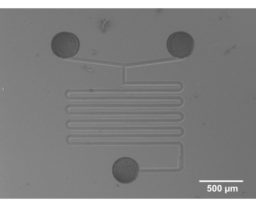
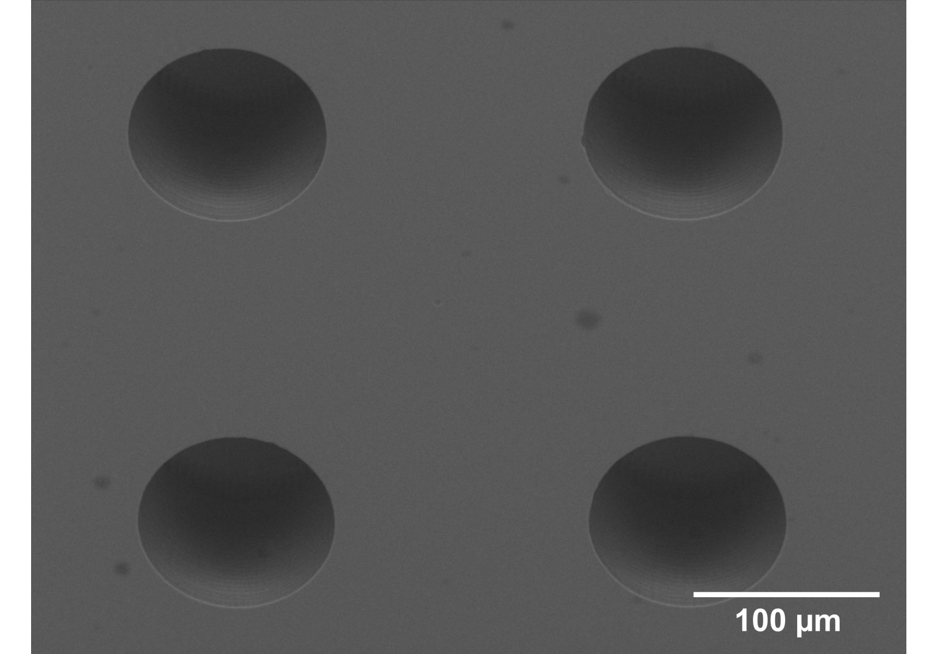
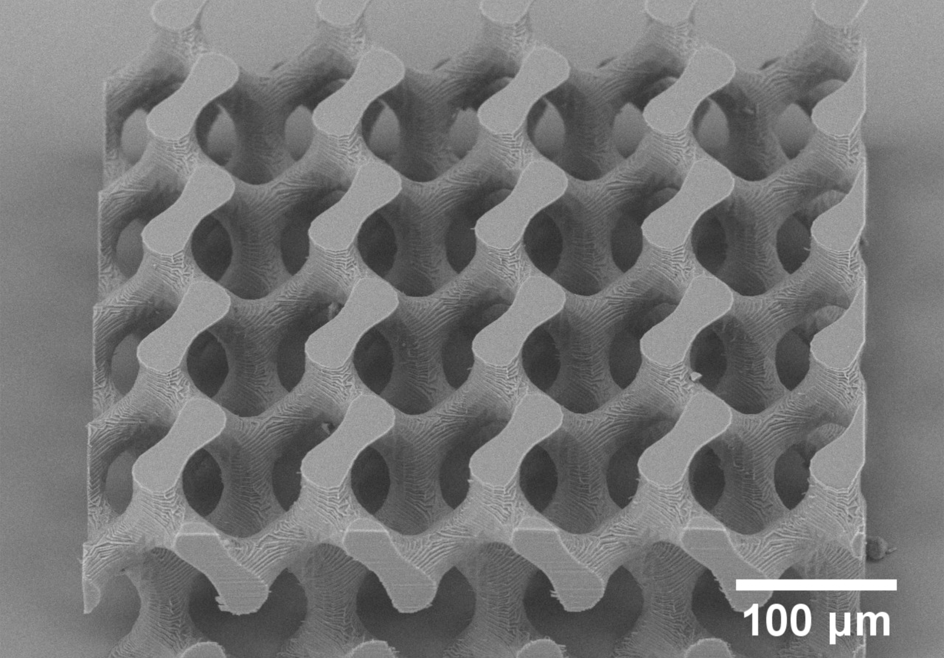
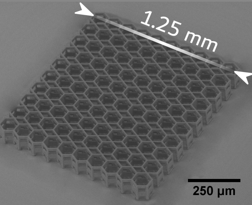
femtika microfluidics

マイクロ流体力学

a液体が非常に狭い空間に閉じ込められた場合には、医薬品の開発・製造、ライフサイエンス、基礎研究などのために非自明な挙動を利用することができます。増幅フェムト秒レーザーは、マイクロ流体部品の製造において非常に有能であることが示されています。任意のフリーフォーム集積素子とボンディングは、たった1台のレーザー微細加工セットアップで実現できます。
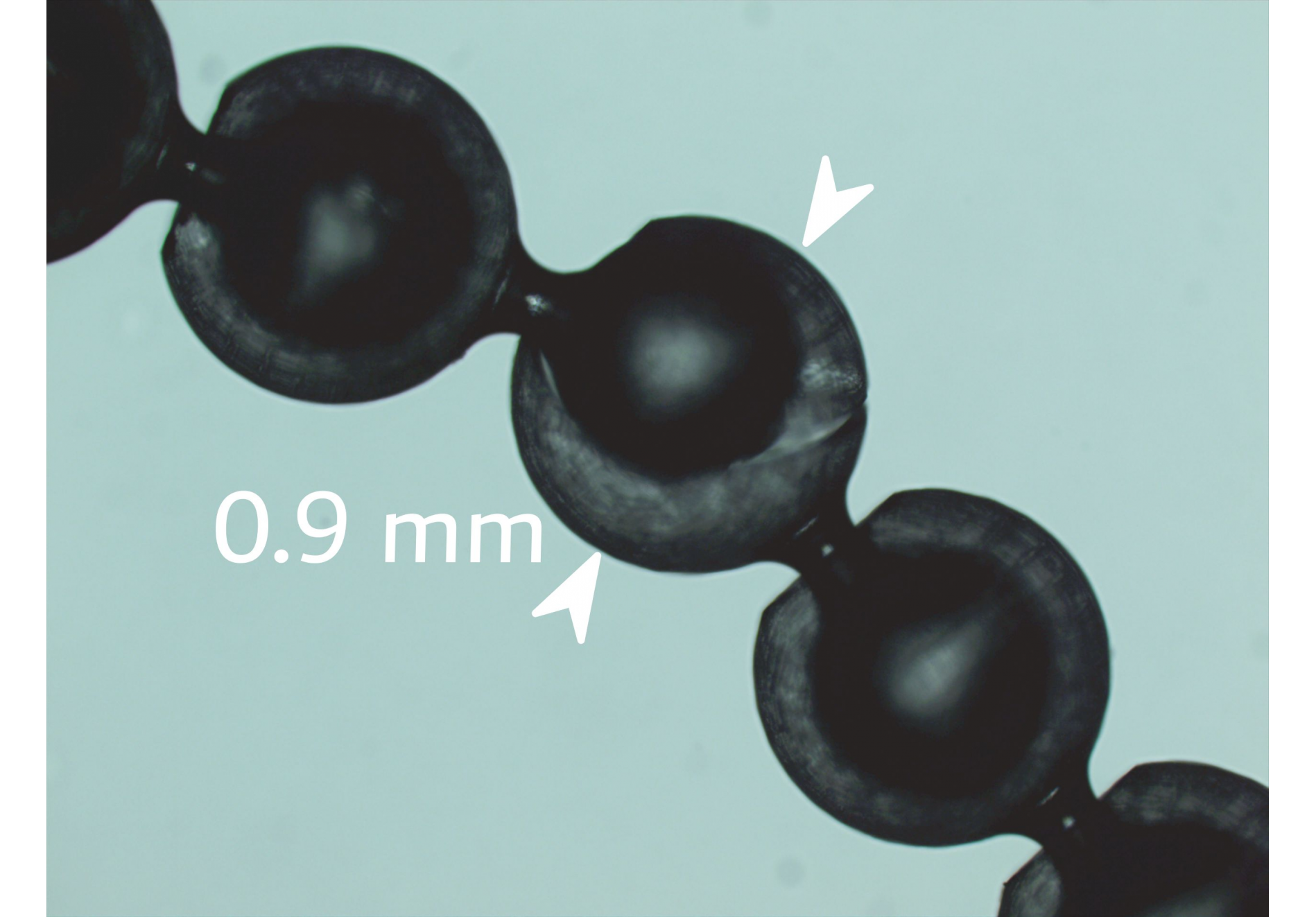
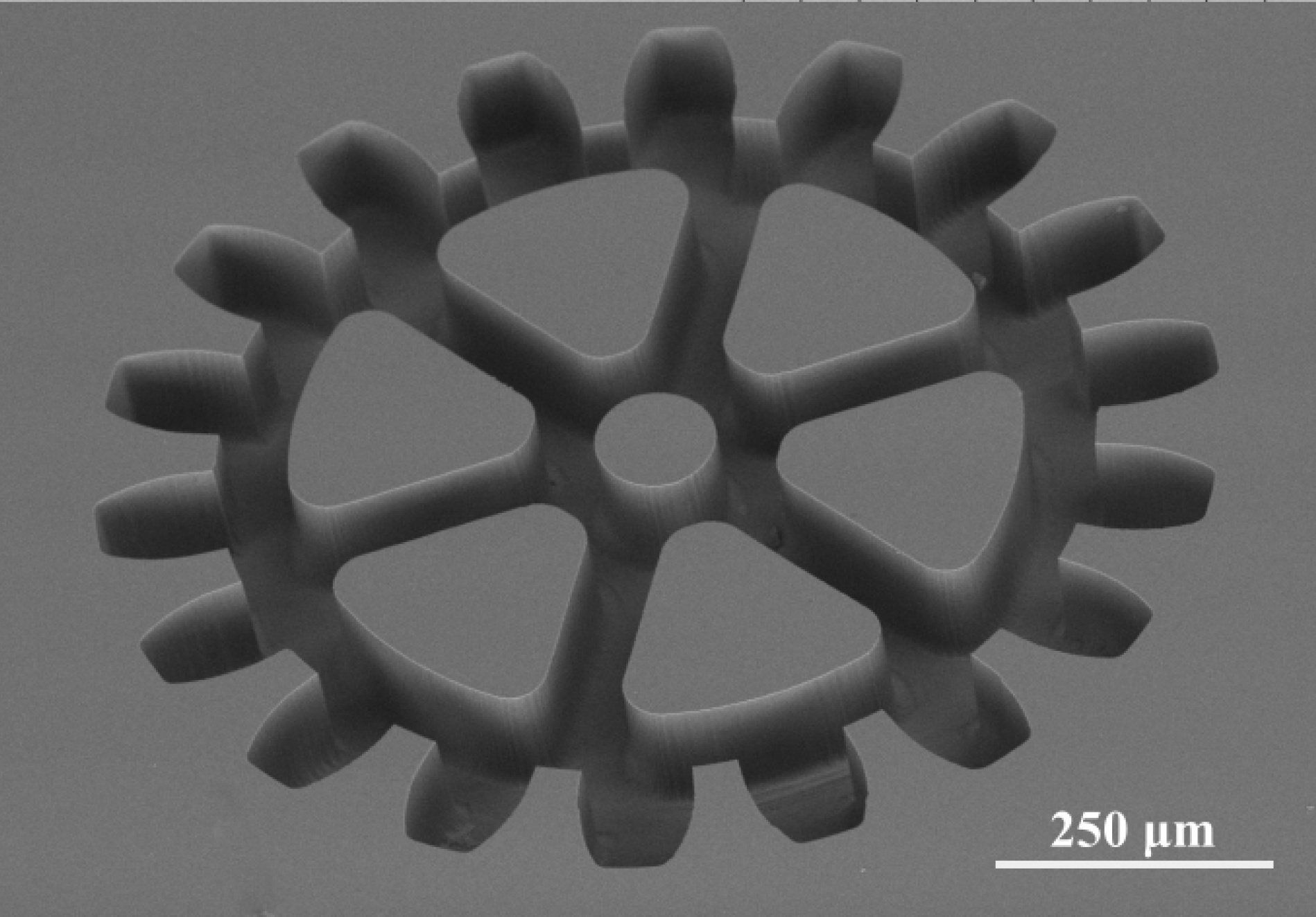
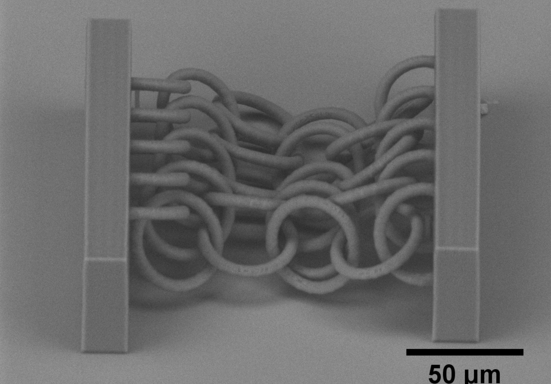
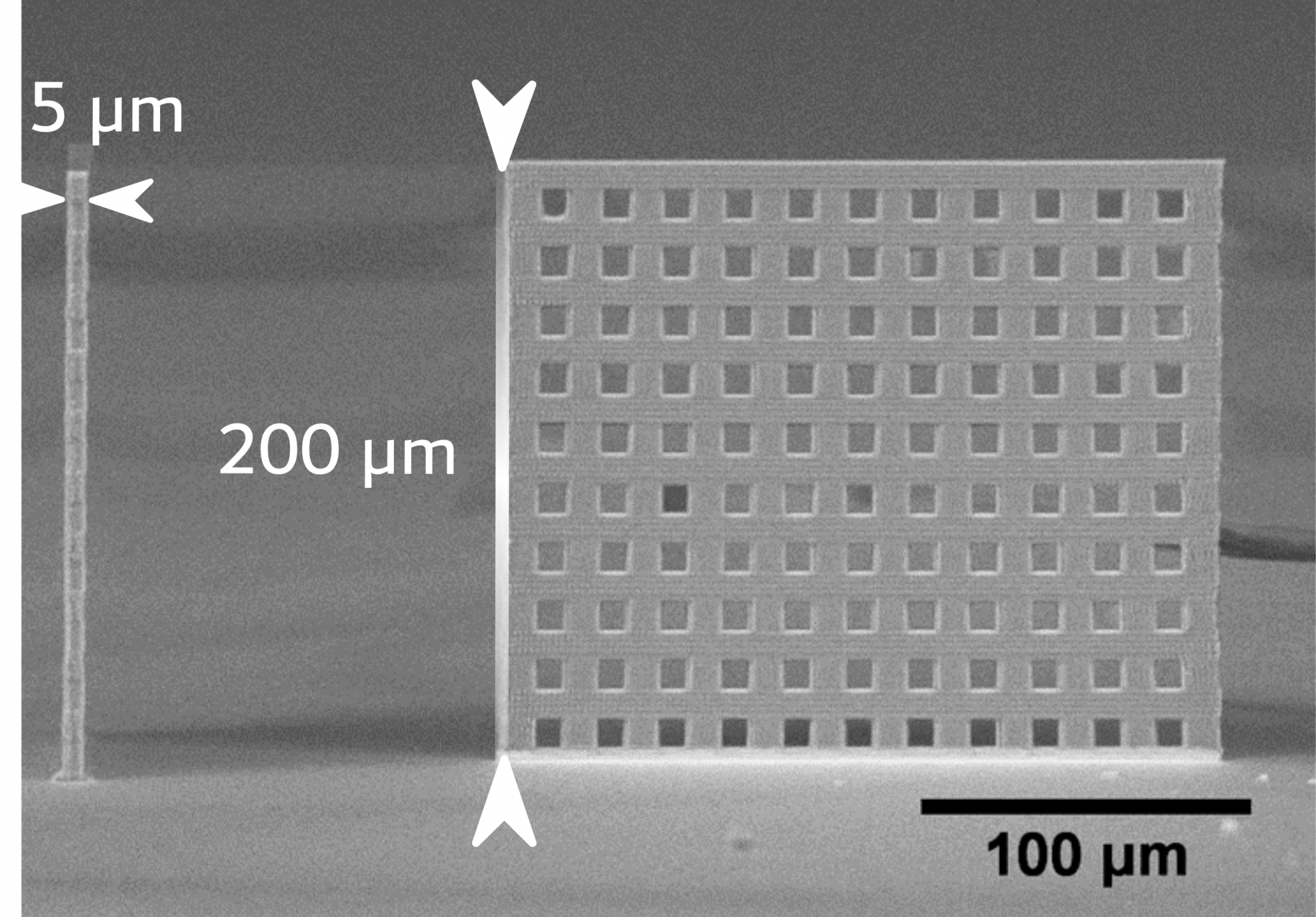
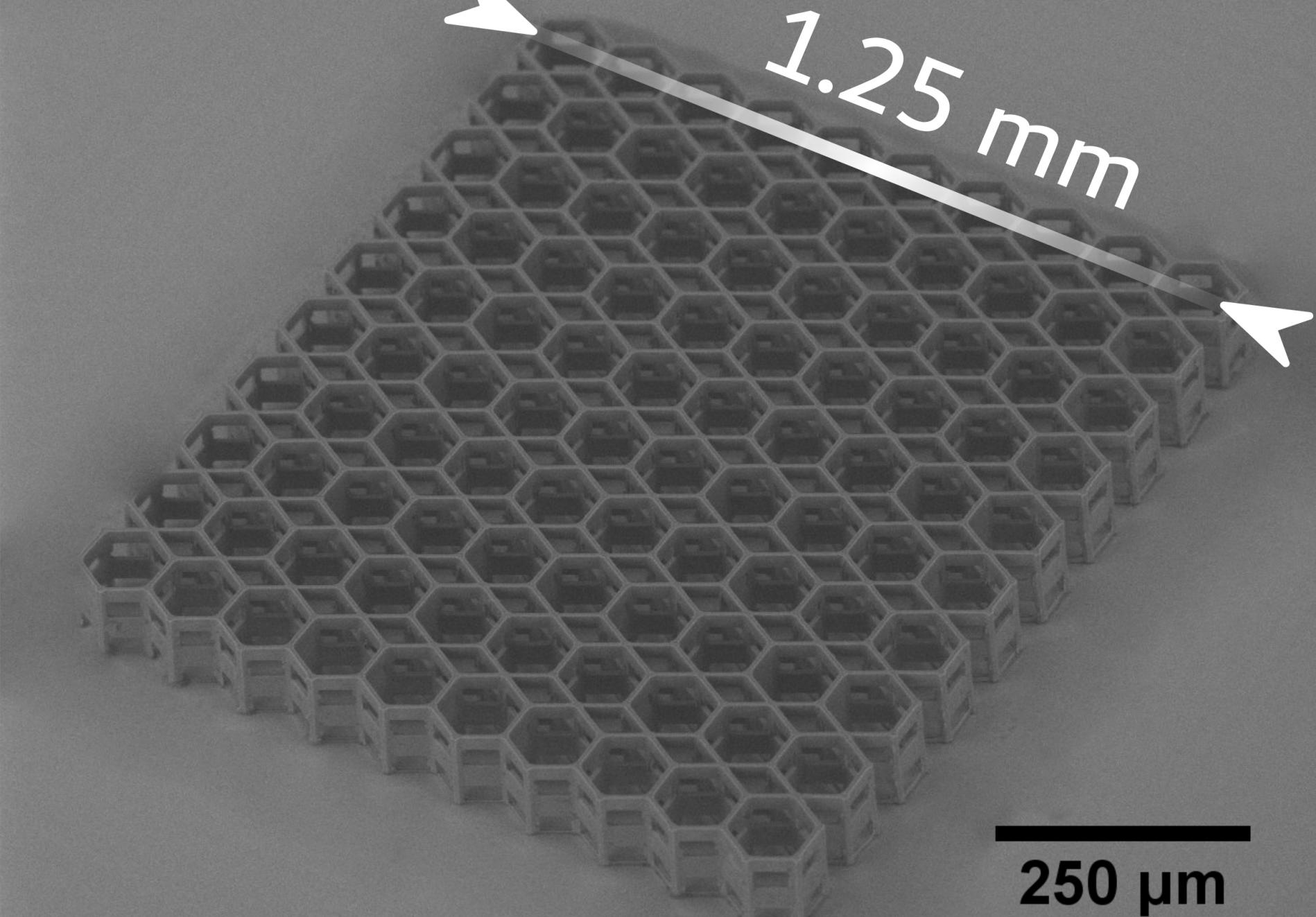
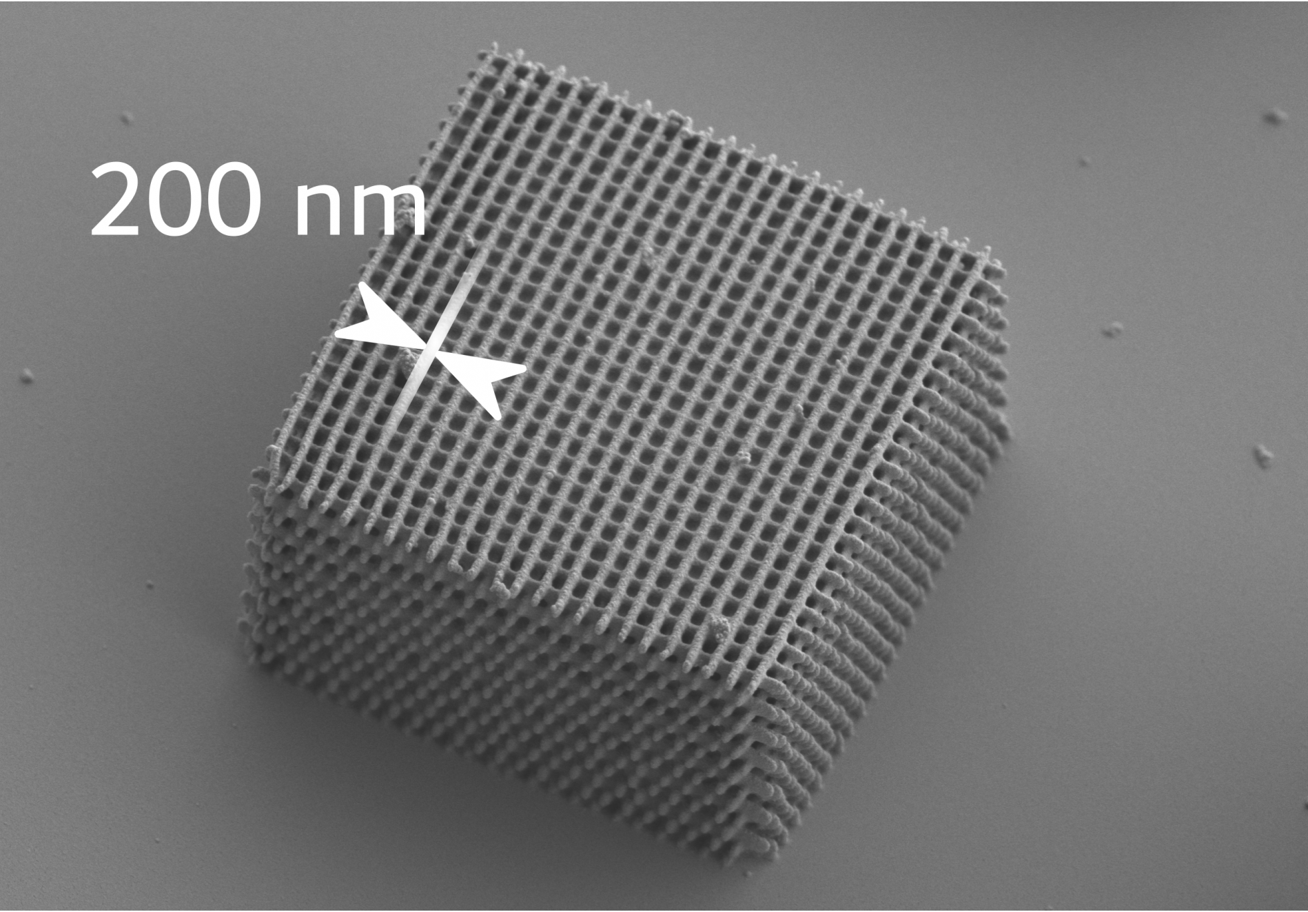
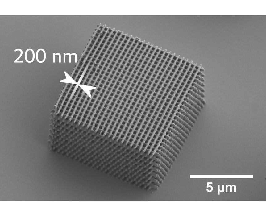
femtika micromechanics

マイクロメカニクス

ナノファクトリーを用いた3Dフェムト秒マイクロマニュファクチャリングでは、サブマイクロメートルスケールの素子を製造することができます。フェムト秒パルスにより、ポリマーやガラス、誘電体結晶、金属など、さまざまな材料を使用した要素の製造が可能になります。歯車、スプリング、カンチレバー、その他の古典的な要素を簡単に作ることができます。
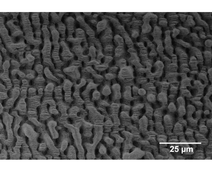
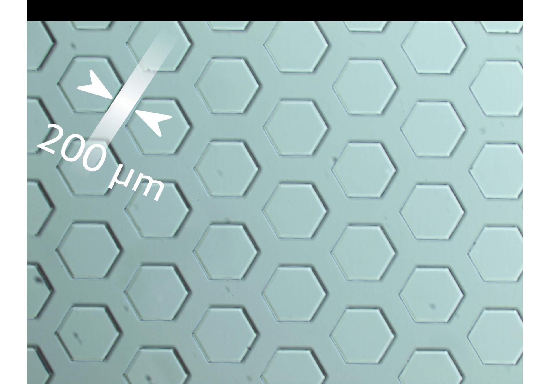
femtika surface structuring

構造化表面

機能性表面は、医療から宇宙開発に至るまで、非常に重要な分野です。fsパルスで作成した表面は、反発性と密着性を両立させた表面を簡単に作ることができます。工具製造、医療用インプラントの抗菌セルフクリーニング面、水による表面摩擦低減、アンチアイシング性など、幅広い応用が可能です。

電子部品

導電性媒体の添加剤層製造が可能で、真の3D電気部品を作成することができます。フェムト秒レーザー加工による熱影響を最小限に抑えることで、電気接点の切断やスクライビングも可能です。レーザーは、電子機器用の高精度基板の製造にも使用でき、溝や穴、その他のパターンをカットすることができます。

ハイブリッド微細加工

fused selica

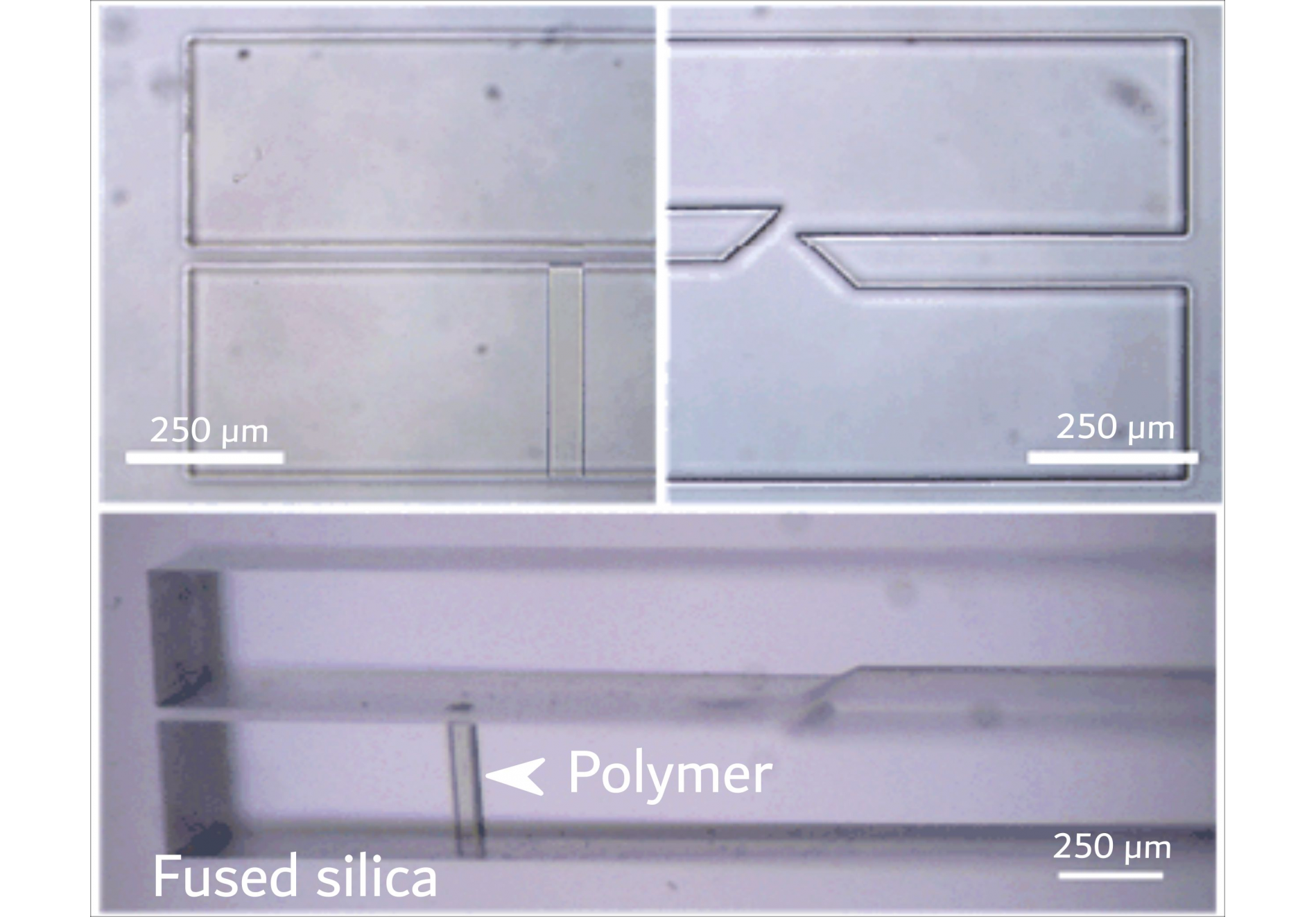
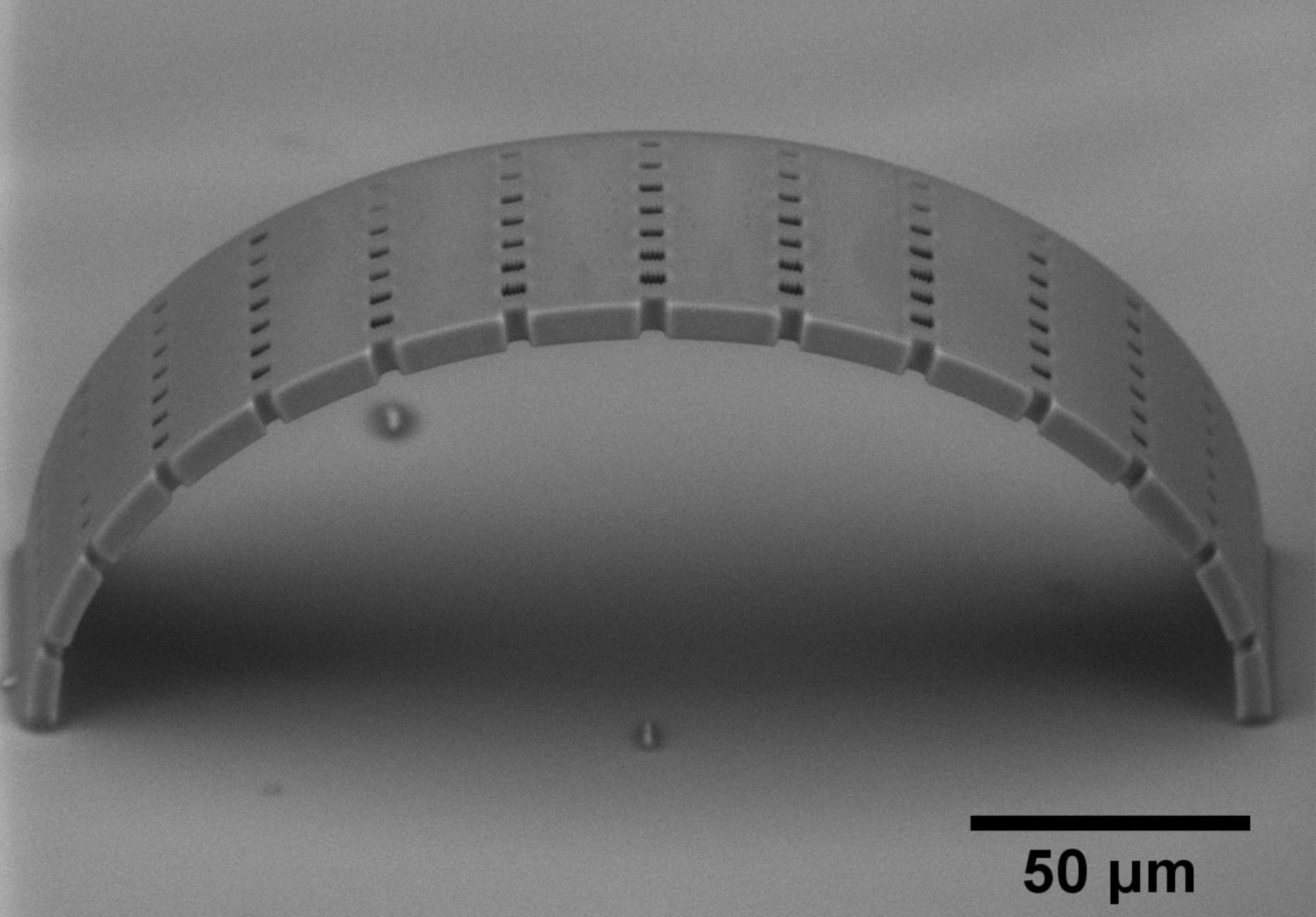
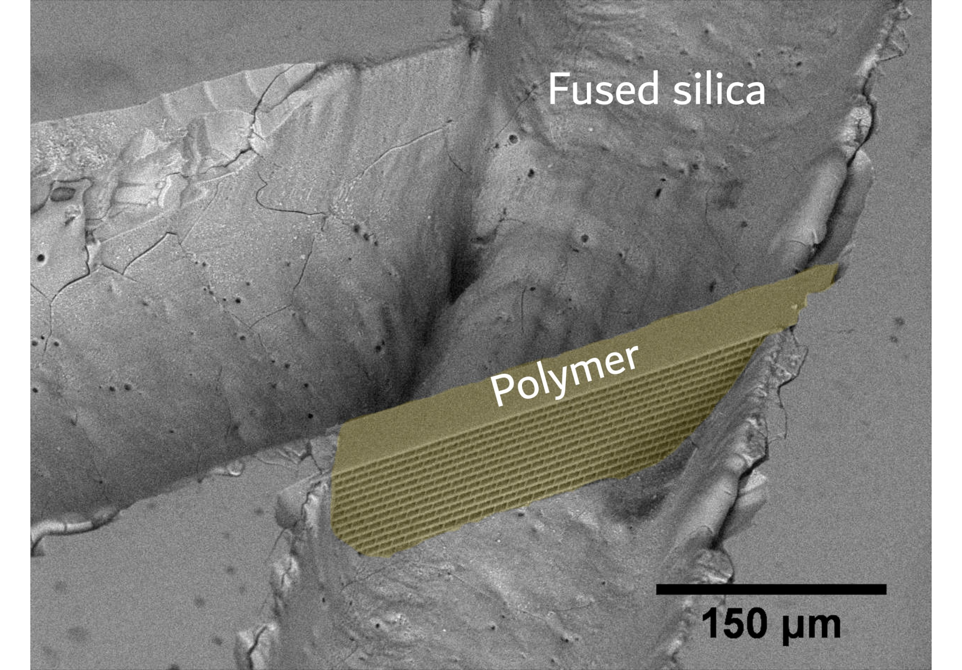
ポリマービームを内蔵した溶融シリカカンチレバー

本製品は、選択的レーザーエッチングと多光子重合を組み合わせて作製しています。重合体ビームは収縮・膨潤によりカンチレバーのたわみを誘発することがあります。
Doi.org/10.1264/OE.25.026280
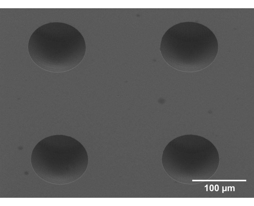
lab-on-chip

ラボオンチップデバイス

ハイブリッド製造の応用により、レーザーアブレーションによる溶融シリカからのチャネルの迅速な製造が可能になります。白色多光子重合を使用して、任意の形状の微細メッシュ3Dフィルターをチャネル内に統合します。システム全体はレーザー溶接で密閉されています。
Doi.org/10.1117/1.OE.56.9.094108


MICRO DEVICE FOR PRECISE DRUG FLOW CONTROL

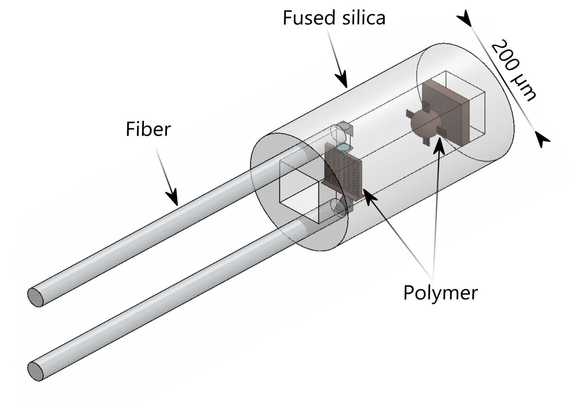
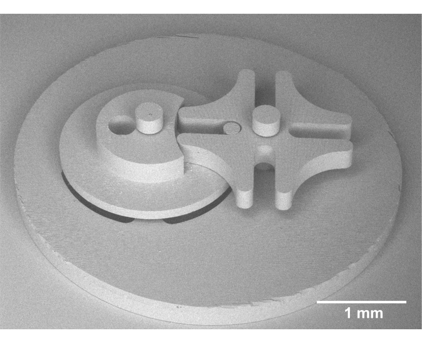
精密ドラッグフロー制御用マイクロデバイス

このデバイスは、カテーテル針、完全に機械的なデバイス、及びオーバーフィルを防止するための統合されたフローシャットオフバルブを備えた光ファイバーを介した高分子カンチレバーの偏向検出を備えた光電子デバイスに統合することができる。重合体要素は、選択的レーザーエッチングを用いて調製された溶融シリカシリンダーに組み込まれている。

選択的レーザーエッチング

サブトラクティブ製造技術、マイクロスケールでの任意形状の3D構造、透明な材料を使用することができます。

多光子重合

マイクロ/ナノスケールでのフォトポリマーの3次元構造化を可能にするダイレクトレーザー書き込み技術。これは、様々な非線形効果の組み合わせ、レーザー放射パラメータの慎重な検討、精密な集光条件によって達成されます。

3DPoli
ソフトウエア・スイート

科学や研究のために特別に作成されたソフトウェア。このような2光子重合、3Dガラス碑文などの装置直接書き込みのセットアップの3次元制御を可能にします。2つの部分で構成されています。

3D Poli Compiler – モーションプロファイルを定義し、実際のシステムとは独立してコンパイルされた命令を生成します。利便性のために他のコンピュータで使用することができます。

3D Poli Fabrication – ライセンスされたシステム上で動作し、コンパイルされたプログラムを実行して構造化されたファブリケーションを実行します。

仕様

レーザー発振器

波長[nm] 1028 nm ± 5 nm
514 nm ± 5 nm
最小パルス幅 <290 fs - 10 ps
最大パルスエネルギー>65 μJ
最大平均出力>4 W
最大繰り返し周波数60 - 1000 kHz
冷却方法空冷式
※上記仕様は全ての項目における最適値の仕様です。
ユーザーのご要望に合わせたカスタム仕様で提案をさせて頂きます。
ご希望の仕様を弊社営業部までお知らせください。

システム

X,Yステージ160 mm x 160 mm
Zステージ60 mm
XYZ直交性3 arc sec
ステージ解像度
1 nm (XY)
2 nm (Z)
ステージ速度
350 mm/s (YX), 200 mm/s (Z)
サンプルホルダーバキューム
14 mm x 66mmの照明領域
5kg以上の負荷の能力
交換が容易なプレート(多孔質セラミック)
寸法高さ1.86 m・幅1.14 m・奥行き0.92 m
※上記仕様は全ての項目における最適値の仕様です。
ユーザーのご要望に合わせたカスタム仕様で提案をさせて頂きます。
ご希望の仕様を弊社営業部までお知らせください。

フェムティカ社製について

Femtikaは、2013年にヴィリニュス大学レーザー研究センターから専門家チームによってスピンオフ企業として誕生しました。彼らは3Dレーザー精密微細加工の研究開発のポートフォリオを持っています。

フェムティカ社製のパートナー

Vikipedija Vilniaus universiteto Fizikos fakultetas

プロジェクト

Project is funded by the European Regional Development Fund, project Nr. 01.2.1-LVPA-K-856, project duration: 2020-2022.

Focused femtosecond radiation allows to selectively induce arbitrary refractive index modulations inside any optical fiber. Additionally, multiphoton polymerization can be used for easy assembly free fabrication of multi-component micro-optical elements on tips of optical fibers allowing to forgo currently used complicated gluing-based multi-step process. Combined,
these two processes will pave the way for a revolution in on-demand fiber-based device manufacturing.

The end goal of the project will be two femtosecond laser-based workstations – one for Brag grating integration into optical fibers and second one for fiber-tip optical element manufacturing.

Prototyping of innovative multifunctional industrial machines for the production of complex microfluidic devices

The aim of the project: to acquire knowledge and form concepts of their application for the development of new microfluidic products for medical and biomedical purposes. Based on them, to develop an efficient technological process for the transfection of microfluidic perforator molecules into cells and the formation of a micro (nano) microfluidic sensor for slow liquid / gas flow. To create prototypes of devices, which will be able to realize the process of laser micro (nano) forming for the layout and production of the mentioned microfluidic products.

During the project implementation period, the following research activities were performed:

1. Investigations of design characteristics and technological concepts of microfluidic channels for cell transfection and fluid flow measurements;

2. Investigations of design parameters and forming concepts of micromechanical components required for cell perforation and fluid flow measurements integrated in microfluidic channels.

Possible essential constructive technological solutions of microfluidic channels were modeled, tested and evaluated during the activity. The optimal solutions have been chosen both in terms of technology, ie simplicity of formation of structures, economy, and functionality in terms of functionality in a medical device. To ensure the functions of the cell perforator, the optimal concept of knives integrated in microfluidic channels was chosen, in the case of a flow meter – the concept based on the use of an electromechanical valve. After refining and finalizing the 3DLL process parameters, it became possible to test and more precisely define the mechanical and optical properties of microfluidic channels and the elements integrated into them, and to use adequate numerical modeling for their design. In this way, it was possible to resolve the scientific uncertainties unknown before the start of the activity.

The objective of project is to develop, test and demonstrate industrial-grade solidstate 2-3 kW-level fs laser with parameters suitable for metal surface patterning for enhanced surface repelling and/or adhesion properties, leading to increased durability, self-cleaning, anti-fouling or enhanced tissue attachment applicable in industrial settings.

FemtoSurf industrial-grade 2-3kW-level fs laser will be integrated in proposebuilt optical chain enabling multi-beam processing (100+ simultaneous beams) with individually tailored spatial distributions in each laser spot, integrated into a fully automated processing setup for efficient patterning arbitrary shaped metal components.

The aim of the project is to deliver the respective enabling technologies of 3D glass micro-nanofabrication for micro chip manufacturing based on a gas handling and delivery system, with an accompanying user interface design for full system automation. The main task is to demonstrate how different geometries and material combinations (metals and oxides) can be combined for production of microchip devices utilised in different types of sensors, e.g. temperature, pressure and capacitive position.

Two types of organic heavy metal free fluorescent materials show exceptional potential for use in new-generation light sources:

i) fluorescence materials exhibiting thermally activated delayed fluorescence (TADF) for use in OLEDs in displays and lighting devices;
ii) fluorescent materials with low thresholds for amplified spontaneous emission (ASE) for use in organic lasers in spectroscopy and telecommunication.
In order to develop these materials for commercial industrial use, the number of the scientific and technical challenges are needed to be overcome.
The overall goal of the MEGA project is to help develop organic heavy metal free fluorescent materials for commercial use by tackling existing scientific and technical challenges.
The aim of the project is to develop an advanced laser beam deflection system for material processing which allows for laser beam positioning pulse by pulse. The system will be able to accelerate several laser processing tasks by a factor of 100 or more. It will be integrated into Femtika‘s next generation Laser Nanofactory workstation. TEM-Messtechnik will develop suitable control equipment. LZH will contribute control and material processing strategies.
The objective of the project is development of the state-of-the-art laser microprocessing by scanning the laser focal point on the material surface. 
The project proposes a new laser lathe approach, including a laser edge interaction, to process objects with rotationally symmetric components. 
For implementation of the project technological and scientific progresses are required on the investigation and application of laser scource, laser shaping, CAD/CAM software, and laser-material interaction.
The Objectives of the project – Development of compact semiconductor laser platform emitting high power/brightness beams. Development a new generation of compact diode laser platforms capable of emitting up to 1kW (without amplifier) with a beam parameter product between 2 and 3 mm·mrad.
LMT Research Group Projects P-MIP-19-444 (2019-2022)
The aim of the project is to create microfluidic nano-microparticle filters using nano-micro scale 3D polymerization, ablation and welding technologies, which would allow continuous fractionation of bio-molecules and bio-particles.
The aim of the project is to develop a cost-effective technology for the production of new advanced spatial filters using thin film coating on nanostructured substrates. The following tasks have been formed for the implementation of the project:
1) To develop the technology of evaporation of multilayer coatings on nanostructured substrates for the formation of photonic spatial filters. 
2) To determine the structural and optical characteristics of the formed elements.
3) To determine the limits of spatial filtration stability of formed elements under laboratory conditions.
4) To confirm the actual operation of the formed elements (prototypes) under laboratory conditions.
The objective of the project is to develop and elaborate feasibility study for Femtika’s developed 3D Micro – nano fabrication device NANOFACTORY commercialization, which would include:
– thorough market research;
– preparation of technical specifications and business plan;
– extensive financial, pricing and IPR strategy.
The aim of the project is to establish a laboratory for the formation of 3D nanostructures of laser polymerization technologies with a high-repetition frequency femtosecond laser system, harmonic generation accessory, nanometric precision three-dimensional displacement system with a galvanometric fiber scanning device. The laboratory equipment is planned to be used for the formation of microstructured three-dimensional structures, micromechanical functional elements, micro-optical elements, research of other laser materials processing technologies.

出版物

メディアとダウンロード